Dies ist eine alte Version des Dokuments!
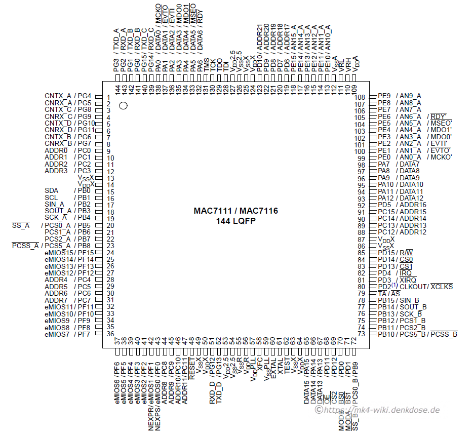
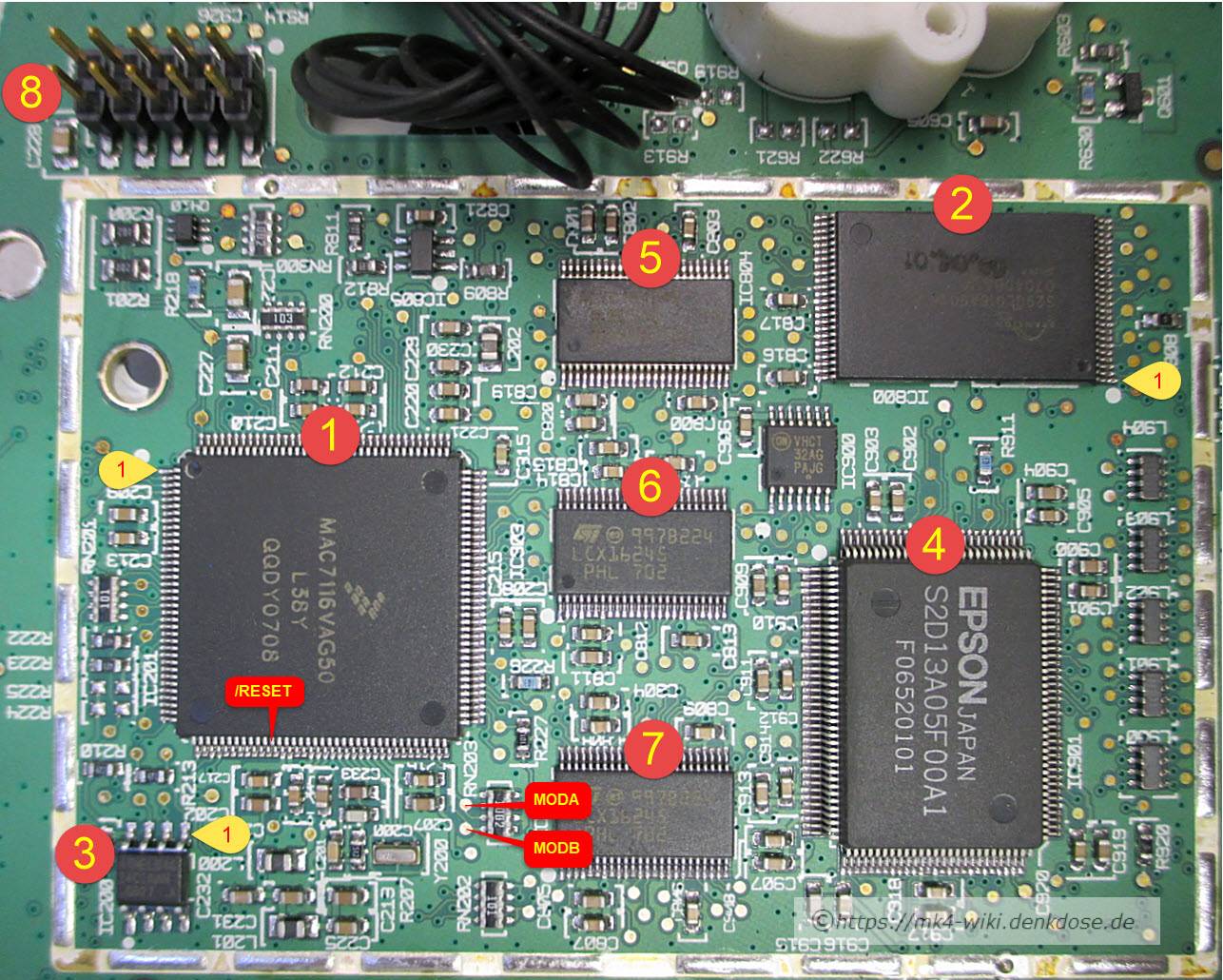
MAC7116 MCU
MCU
- Bauteileschriftung:
NXP MAC7116VAG50 - Gehäuse: 144LQFP
- CPU: ARM7
- Core: ARM7TDMI-S:
- 32 Bit Big-Endian
- ARMv4T Instruction-Set
- 50 MHz Clock
- 8kb unified cache
- Memory Management Unit (MMU)
- EmbeddedICE macrocell consists of on-chip logic to support debug operations via JTAG-Interface
- The core is implemented to support big-endian memory systems.
- Quartz: 8 MHz
- Program Flash: 1 MByte
- Data Flash: 32 KByte
- SRAM: 48 KByte
- Datenblatt: https://www.nxp.com/part/MAC7116VAG50
Bootstrap
Chip operation mode
The chip operating mode is determined by the states of the MODA (Pin 71) and MODB (Pin 70) pins at reset and the security status of the program Flash.
| MODA | MODB | Program Flash secured | Chip mode | Description |
|---|---|---|---|---|
| 0 | 0 | No | Normal Single-Chip Mode | Boots from internal flash |
| 0 | 1 | No | Normal Expanded Mode | Boots from external flash |
| 1 | 0 | No | Normal Data Flash Boot Mode | Boots from data flash |
| 0 | 0 | Yes | Secured Single-Chip Mode | Boots from internal flash |
| 0 | 1 | Yes | Secured Expanded Mode | Boots from external flash |
| 1 | 0 | Yes | Secured Data Flash Boot Mode | Boots from data flash |
| 1 | 1 | - | -RESERVED - |
Memory Map
| Periphal | Base-Addr | End-Addr | Size |
|---|---|---|---|
| Program Flash | 0x0000 0000 | 0x000F FFFF | 0x10 0000 (1 mb) |
| Data Flash | 0xFE00 0000 | (32 kb) | |
| SRAM | 0x4000 0000 | 0x4000 7FFF | 0x8000 (48 kb) |
progflash base 0xfc100000
JTAG

- No RTCK
- JTAG-Speed: 750 or 1.000 KHz (fixed)
- VTref = 5.0 Volt
- Code-ID: 0x4F1F0F0F
- IR-Len: 4 Bit
- IR-Print: 0b0001 (0x01)
- Target RAM: 48 KByte @ 0x4000 0000
- MCU Init procedure:
- Reset:
- Type ⇒ 0
- Delay ⇒ 20 ms
- Device complying to IEEE 1149.1 JTAG standard.
- JTAG IR and DR Sequence: JTAG Instruction Register (IR) scan to load an opcode value for selecting a development register. The selected development register is then accessed via a JTAG Data Register (DR) scan.
- Embedded-ICE: The ARM7 EmbeddedICE debug module. This module integrated with each ARM7 processor provides all static (core halted) debug functionality. This module is compliant with Class1 of the IEEE-ISTO 5001 standard.
External Interface Module (EIM) Configuration Registers
Address range: 0xFC00 8000 – 0xFC00 BFFF
CFM Flash Configuration Field
| Address Offset from PROGRAM FLASH BASE | Size | Function | Factory Default |
|---|---|---|---|
| 0x0400 – 0x0407 | 8 | Backdoor Comparison Key | 0xFFFF_FFFF_FFFF_FFFF |
| 0x0408 – 0x040B | 4 | Program Flash Protection Bytes | 0xFFFF_FFFF |
| 0x040C – 0x040F | 4 | Program Flash SUPV Access Bytes | 0xFFFF_FFFF |
| 0x0410 – 0x0413 | 4 | Program Flash DATA Access Bytes | 0xFFFF_FFFF |
| 0x0414 – 0x0417 | 4 | Flash Security Word Section | 0xFFFF_FFFF |
| 0x0418 | 1 | Data Flash Protection Byte Section | 0xFF |
| 0x0419 | 1 | Data Flash SUPV Access Byte Section | 0xFF |
| 0x041A | 1 | Data Flash DATA Access Byte Section | 0xFF |
CFM Registers and values
Address Range: 0xFC0F 0000 – 0xFC0F 3FFF
CFM Clock Divider Register (CFMCLKD)
| Register | Address | Size |
|---|---|---|
| CFMCLKD | 0xFC0F 0002 | 8 Bits |
The CFMCLKD register is used to control the period of the clock used for timed events in program anderase algorithms. All CFMCLKD register bits are readable while bits [6:0] are write once and bit 7 is notwritable.
The CFMCLKD register bits PRDIV8 and DIV must be set with appropriate values before programming or erasing the CFM Flash memory.
CFM-Command "Mass Erase Flash" (0x41)
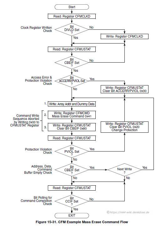
Init procedure
DEFs
;	MM	memory mapped register
;name		type	addr		size
cfmmcr  	MM	0xFC0F0000	16
cfmclkd 	MM	0xFC0F0002	8
cfmsec  	MM	0xFC0F0008	32

cfmprot 	MM	0xFC0F0010	32

cfmsacc 	MM	0xFC0F0014	32
cfmdacc 	MM	0xFC0F0018	32
cfmustat	MM	0xFC0F0020	8
cfmcmd  	MM	0xFC0F0024	8
cfmdfprot       MM	0xFC0F0044	8
cfmdfsacc       MM	0xFC0F0045	8
cfmdfdacc       MM	0xFC0F0046	8
Segger
w1 FC0F0020,0xFF // Clear viol flag
w1 FCOF0044,0x00 //unlock data flash write protection
w2 FE000000,0x1234 //Write half-word to init write procedure
w1 FCOF0024,0x20 //write WRITE command
w1 FCOF0020,0x80 //write flag to start procedure
mem16 fe000000,1 // verify writing->FE000000=FFFF // write fault
PEEDI
;-------------------------------------------------------------------------------
;
;
;   PEEDI target configuration file for Freescale MAC7100 processor
;
;   Ronetix
;
;   Supported devices   : MAC7100
;
;   Revision            : 1.5
;
;   Date                : March 23, 2007
;
; The software is delivered "AS IS" without warranty or condition of any
; kind, either express, implied or statutory. This includes without
; limitation any warranty or condition with respect to merchantability or
; fitness for any particular purpose, or against the infringements of
; intellectual property rights of others.
;
;-------------------------------------------------------------------------------

;--------------------------------------------------------------------------
; The following section contains licenses that are required for PEEDI to
; operate. These licenses must be filled before using this file.
; The [LICENSE] section may contain license keys for one or more PEEDIs.
;
;   Example:
;       [LICENSE]
;       KEY         = UPDATE_24MAY2010, 1111-1111-1111-1
;       KEY         = XXXXX, 2222-2222-2222-2
;
; The [LICENSE] section may point to an external file which contains
; license keys for one or more PEEDIs. The external file must include
; the text [LICENSE] followed by all keys.
;
;   Example:
;		[LICENSE]
;		FILE = tftp://192.168.3.1/license.txt
;		or
;		FILE=eep:license.txt
;		or
;		FILE = ftp://user:password@192.168.3.1/license.txt
;
;
; PEEDI is shipped with license keys stored in "eep:license.txt" and
; printed on a label on the bottom side of PEEDI.
;
[LICENSE]
FILE=eep:license.txt
;--------------------------------------------------------------------------

[DEBUGGER]
PROTOCOL            = gdb_remote            ; gdb remote
REMOTE_PORT         = 2000                  ; TCP/IP port

[TARGET]
PLATFORM            = ARM                   ; platform is ARM

[PLATFORM_ARM]
JTAG_CHAIN          = 4                     ; list of IR length of all TAP controller in JTAG chain
JTAG_CLOCK          = 20, 4000              ; JTAG Clock in [kHz] - 10kHz jtag clock for init operations and 4MHz for normal work
                                            ; Freescale recommends max JTAG_CLOCK 1/6 of the system clock
TRST_TYPE           = OPENDRAIN             ; type of TRST output: OPENDRAIN or PUSHPULL
RESET_TIME          = 20                    ; 20ms reset pulse, 0 means no reset
TIME_AFTER_RESET    = 100                   ; time between releasing the reset and starting the jtag communication
CORE0               = MAC7100               ; TAP is Freescale MAC71xx  CPU
CORE0_STARTUP_MODE  = RESET                 ; startup mode after reset:
                                            ;   if RESET than no code is executed after reset
                                            ;   if STOP,XX then the target executes code for XX period in ms.
                                            ;   if RUN then the target executes code until stopped by the telnet "halt" command

CORE0_BREAKMODE         = soft              ; breakpoint mode:
                                            ; soft - software breakpiont
                                            ; hard - use hardware breakpoints instead of software
CORE0_BREAK_PATTERN     = 0xDFFFDFFF        ; software breakpoint pattern

CORE0_INIT              = INIT_MAC7100      ; init section for MAC7100 board
CORE0_FLASH0            = FLASH_PROG        ; PROGRAM flash section parameters
CORE0_ENDIAN            = BIG               ; core is big endian
CORE0_WORKSPACE_ADDR    = 0x40000100        ; start address of workspace for flash programmer
CORE0_WORKSPACE_LEN     = 0x4000            ; length of workspace in bytes

CORE0_LOCKOUT_RECOVERY  = 19                ; If this parameter is present, PEEDI automatically executes a
                                            ; "JTAG Lockout Recovery" procedure during reset processing
                                            ; if the MAC7100 flash is secured
                                            ; Fsys 4MHz CLKD=9; Fsys 8MHz CLKD=19
CORE0_FILE              = "myfile.bin", BIN, 0x40000100 ; default file
CORE0_PATH              = "tftp://192.168.3.1" ; default path

[INIT_MAC7100]
memory write8  0xfc088004 0     ; CRGINT Disable clock interrupts

; Speed-up to fsys = 50MHz, Fsys = 2*Fosc*(mul/div)
; Quartz is 8.00 MHz
;--------------------------------------------------
memory write8  0xfc088001 0x07          ; REFDV - CRG Reference Divider register - divide by 8
memory write8  0xfc088000 0x18          ; SYNR - CRG synthesizer Register - multiply by 25
wait 10
memory write8  0xfc088005 0x80          ; CLKSEL - Select fsys=PLLCLK
memory write8  0xFC088003 0x72          ; clear the flags

memory write8  0xfc088008 0x00          ; BDMCTL - SWT and RTI keep running in debug mode
memory write16 0xfc0e80c4 0x0080        ; output CLKOUT on PD2

set pc 0x40000000                       ; set PC to RAM memory base

[FLASH_PROG]
CHIP                = MAC7100           ; flash chip
CPU_CLOCK           = 50000             ; PLL clock
CHECK_ID            = YES
FILE                = "myprog.bin", BIN, 0xFC100000 ; file to program
AUTO_ERASE          = NO               ; erase before program


[SERIAL]                                ; serial port configuration
BAUD                = 115200
STOP_BITS           = 1
PARITY              = NONE
TCP_PORT            = 0                 ; enable CLI over RS232
;TCP_PORT           = 2023              ; enable serial over TCP/IP

[TELNET]
PROMPT              = "MAC7100> "       ; telnet prompt
;BACKSPACE          = 127               ; comment out for autodetect

[DISPLAY]
BRIGHTNESS          = 20                ; LED indicator brightness
VOLUME              = 25                ; zummer volume

[ACTIONS]                               ; user defined scripts
1 = erase
2 = prog
3 = dump_ram
4 = dump_flash

[erase]                                 ; erase flash
flash erase

[prog]                                  ; program flash
flash prog
...
; bdiGDB configuration file for MAC7100 EVB
; -----------------------------------------
; CS0 selects 128k SRAM  @ 0x00000000
; CS1 selects  2MB Flash @ 0x01000000
; CS2 not used
; CLOCK OUT is 8.00 MHz
;
[INIT]
; Setup memory controller
WM16    0xFC008080  0x0000	;CSAR0: CS0 at 0x00000000
WM16    0xFC00808A  0x15A0	;CSCR0: CS0 5 waits, 16bit
WM32    0xFC008084  0x001F0001	;CSMR0: CS0 2MB, R/W, valid
WM16    0xFC00808C  0x0100	;CSAR1: CS1 at 0x01000000
WM16    0xFC008096  0x15A0	;CSCR1: CS1 5 waits, 16bit
WM32    0xFC008090  0x001F0001	;CSMR1: CS1 2MB, R/W, valid
WM16    0xFC008098  0x0200	;CSAR2: CS2 at 0x02000000
WM16    0xFC0080A2  0x15A0	;CSCR2: CS2 5 waits, 16bit
WM32    0xFC00809C  0x001F0001	;CSMR2: CS2 2MB, R/W, valid
;
; Enable internal flash programming
WM32    0xFC0F0010  0x00000000	;CFMPROT  : disable code flash protection
WM8     0xFC0F0044  0x00      	;CFMDFPROT: disable data flash protection
;
;
; Speed-up to fsys = 50MHz
WM8     0xFC088001  0x07      	;REFDV : divide   by 8
WM8     0xFC088000  0x18      	;SYNR  : multiply by 25
DELAY   100                     ;let the PLL lock
WM8     0xFC088005  0x80      	;CLKSEL: Select PLL
WM8     0xFC088003  0x72      	;CRGFLG: Clear the flags
;

[TARGET]
CPUTYPE     MAC7100
CLOCK       3 5                 ;select 4MHz JTAG clock, init with 500kHz
DEBUGPC     0x40000000          ;set save PC to internal SRAM
ENDIAN      BIG                 ;memory model (LITTLE | BIG)
BREAKMODE   SOFT 0xDFFFDFFF     ;SOFT or HARD, ARM / Thumb break code
;VECTOR      CATCH
;DCC         7                   ;DCC I/O via TCP port 7

[HOST]
IP          151.120.25.119
FILE        E:\cygwin\home\demo\pid7t\fibo.x
FORMAT      ELF
LOAD        MANUAL    ;load code MANUAL or AUTO after reset

[FLASH]
; External Flash at 0x01000000
; ============================
;WORKSPACE   0x40000000         ;workspace in internal SRAM for fast programming algorithm
;CHIPTYPE    AM29BX16           ;Flash is AM29F160DB
;CHIPSIZE    0x200000           ;The size of one flash chip in bytes
;BUSWIDTH    16                 ;The width of the flash memory bus in bits (8 | 16 | 32)
;FILE        E:\cygwin\home\bdidemo\arm\mac7100.cfg  ;The file to program
;FORMAT      BIN 0x01000000
;ERASE       0x01000000         ;erase sector 0
;ERASE       0x01004000         ;erase sector 1
;ERASE       0x01006000         ;erase sector 2
;ERASE       0x01008000         ;erase sector 3
;ERASE       0x01010000         ;erase sector 4
;ERASE       0x01020000         ;erase sector 5
;ERASE       0x01030000         ;erase sector 6
;ERASE       0x01040000         ;erase sector 7
;ERASE       0x01050000         ;erase sector 8
;ERASE       0x01060000         ;erase sector 9
;ERASE       0x01070000         ;erase sector 10
;
; Internal Program Flash at 0xfc100000
; ====================================
WORKSPACE   0x40000000          ;workspace in internal SRAM for fast programming algorithm
;CHIPTYPE    CFM32 8000          ;select Program flash, fsys = 8MHz
CHIPTYPE    CFM32 50000         ;select Program flash, fsys = 50MHz
CHIPSIZE    0x80000             ;512k internal program flash
BUSWIDTH    32                  ;The width of the flash memory bus in bits (8 | 16 | 32)
RECOVER     19                  ;Do JTAG lockout recovery if necessary, CLKD for fsys = 8MHz
FILE        E:\cygwin\home\bdidemo\arm\mac7100.cfg  ;The file to program
FORMAT      BIN 0xfc101000      ;do not secure the device !!!
;ERASE       0xfc100000 PAGE     ;erase page 0 (security byte will be restored)
ERASE       0xfc101000 PAGE     ;erase page 1
ERASE       0xfc102000 PAGE     ;erase page 2
ERASE       0xfc103000 PAGE     ;erase page 3
;ERASE       0xfc100000 MASS     ;mass erase (security byte will be restored)
;
; Internal Data Flash at 0xfe000000
; =================================
;WORKSPACE   0x40000000          ;workspace in internal SRAM for fast programming algorithm
;CHIPTYPE    CFM16 8000          ;select Data flash, fsys = 8MHz
;CHIPTYPE    CFM16 50000         ;select Data flash, fsys = 50MHz
;CHIPSIZE    0x8000              ;32k internal data flash
;BUSWIDTH    16                  ;The width of the flash memory bus in bits (8 | 16 | 32)
;FILE        E:\cygwin\home\bdidemo\arm\mac7100.cfg  ;The file to program
;FORMAT      BIN 0xfe000000
;ERASE       0xfe000000 PAGE     ;erase page 0
;ERASE       0xfe000400 PAGE     ;erase page 1
;ERASE       0xfe000800 PAGE     ;erase page 2
;ERASE       0xfe000c00 PAGE     ;erase page 3
;ERASE       0xfe001000 PAGE     ;erase page 4
;ERASE       0xfe001400 PAGE     ;erase page 5
;ERASE       0xfe001800 PAGE     ;erase page 6
;ERASE       0xfe001c00 PAGE     ;erase page 7
;


[REGS]
FILE	E:\cygwin\home\bdidemo\arm\reg7100.def
NEXUS Port
The MAC7100 family of devices offers debugging with the Embedded ICE (E-ICE) and a NEXUS 2 Plus interface of the core. Embedded ICE offers debug features such as setting breakpoints or watchpoints, modifying and reading memory contents. Embedded ICE uses the standard JTAG serial interface and Test Access Port (TAP) and is compatible with existing ARM7 tool chains. The NEXUS interface provides real time program trace capability and also uses the JTAG port, as well as providing an auxiliary port.
Security
MAC7100 Family devices implement a security feature that prevents the unauthorized read and write of the memory contents. This feature allows:
- Protection of the contents of program Flash
- Protection of the contents of data Flash
- Operation in single-chip mode
- Operation from external memory with internal program Flash and data Flash disabled
Programmers developing code for MAC7100 Family devices must be aware that part of the security mechanism is the responsibility of the user’s code. An extreme example of defeating the security mechanism would be user code that dumps the contents of the internal Flash to external memory or an I/O port. However, the user may also wish to put a back door in the application code. For example, in order to update parameters stored in Flash, a routine might be developed to allow the download of a security key through the eSCI, allowing access to a programming routine.
Once the user has written the contents of the program Flash and data Flash (if desired), the device can be secured by programming the security bits located in the Flash module CFM Security Register (CFMSR, refer to Figure 15-8 on page 15-217). These non-volatile bits will keep the part secured through resets and power down.
When security is enabled both the program and data Flash memories are secured, it is not possible to configure security independently for these two memory types. The Flash Memory Security Bits of the CFMSR contain the setup for the controlling access to the Flash memories and resides in an area of the Flash array.
Unlock
IMPORTANT: if the CFM Flash Configuration Field (0x400 – 0x41B) is (over)written with user program, it is highly likely that the device will be secured AFTER the next RESET.
If the CFM is accidentally secured, use the following procedure to unsecure the device:
- Switch off the power to the target and emulator.
- Force the MAC7100 to boot in single chip (set MODA and MODB pins to 0)
- Turn on the emulator and the target
- Select Hardware/FLASH/Unsecure
With some specific values a different kind of protection can occur (the debugger will fail to initialize without error message) – use these steps:
- Switch off the power to the target and emulator.
- Force the MAC7100 to boot in expanded mode (set MODA to 0 and MODB pin to 1)
- Turn on the emulator and the target
- Make sure FLASH/Setup/Scope/Entire chip is selected
- Select FLASH/Program/Erase.
JTAG Lockout Recovery
If the Flash security is enabled, the only way to unlock the device is to perform JTAG Lockout Recovery procedure.
Utilize the JTAG interface to perform a lockout recovery. In a manner similar to ARM CPU instruction execution flows described in Section 15.4.1.5, “Program, Erase, and Verify Operations,” a sequence of JTAG commands can be used to:
- Execute a mass erase command
- execute a blank check,
- program the Flash Security Word (offset 0x0414) bits corresponding to the CFMSEC[SEC] field to 0b10 (see Section 15.3.1.3)
- RESET the device into expanded mode to execute boot code from external memory.
Refer to Section B.4.4.3, “Memory Mapped Register Access via JTAG,” on page B-612 for more information on using the JTAG interface to read and write memory-mapped CFM module registers.
Security bits in program Flash range
In program FLASH the address range from 0x0400 to 0x041F is used to set the FLASH security. If there is user code this could secure the FLASH incidentally, so avoid placing code there!
flash erase chip - perform MASS ERASE
flash lock- write at address 0xFC100414 = 0xFFFFFFFC0 (enable flash security)
PEEDI executes a ’JTAG Lockout Recovery’ during reset processing if the MAC7100 flash is secured and if the configuration file contains: CORE_LOCKOUT_RECOVERY = clkd
1 MByte Program Flash address is depending on Operation mode.
;   Expanded:            0x20000000--0x200fffff
;   Single Chip:         0x00000000--0x000fffff
;   Program interface:   0xfc100000--0xfc1fffff
; 32 kByte Data Flash at 0xfe000000--0xfe007fff
; 48 kByte RAM at        0x40000000--0x4000bfff
;
; Optional argument unsecure is used to a unsecure a secured chip.
;
; Optional argument unlock is used to a reset LOCK bit of CFMMCR register.
;
; HINTS:
;   Security word only can be written by a explicit data set to that
;   location, for example "Data.Set 0xfc100414 %Long 0x80000000".
;   All other operations do not allow securing the device. The two security
;   bits are forced to unsecure value.
;
;   Program and data flash have same unit number in flash declaration because
; mass erase does erase program and data flash.