OMAP5948
Hintergrundinfos
The OMAP5948 is used in several Blaupunkt (a brandname of Automotive products from the Bosch Company) Radio-Navigationsystems. „OMAP“ is a shortcut for „Open-Multimedia-Application-Platform“. It stands for a series of Microcontrollers (SoC = System-On-Chip) of Texas Instruments (TI). It is part of the „OMAP-1“ Family (https://en.wikipedia.org/wiki/OMAP), but never sold for end customers. It's datasheet is under NDA, so you will not find it in public. All my investigations showed that it is a special variant of the OMAP5912 with some „custom extensions“ made for Bosch. For the OMAP5912 you find plenty of information, available for free.
If somebody ever get's his hands on an real OMAP5948 datasheet, please contact me via the Contact-Form !
SOC-Aufbau
Der Chip enthält neben einer ARM-CPU und einem DSP auch noch viele weitere Komponenten, wie diese Blockgrafik verdeutlicht:

Nicht alle davon kommen in den Navigationssystemen zum Einsatz. Die Betriebs- und Signal (IO) Spannung beträgt 1,6V und der Chip kann mit maximal 192 MHz getaktet werden. Da für die internen Komponenten nicht jeder Pin einzeln rausgeführt wird, sind etliche Pins im „Multiplex“ belegt. D.H. je nach Softwarekonfiguration des Chips kann der Pin eine andere Funktion haben. Erkennbar ist dies an Pinbezeichnungen die durch Schrägstrich getrennt sind, z.B. MPUIO1/RTCK/SPIF.SCK. Dieser Pin könnte also intern entweder mit einem generischen IO-Port der CPU (MPUIO1), einem Signal des JTAG-Controllers (RTCK) oder mit dem Taktsignal einer SPI-Schnittstelle (SPIF.SCK) verbunden sein.
Dieses Schaubild zeigt einen funktionalen Überblick des Chips:

Die ARM-CPU (MPU)
Der CPU im OMAP entspricht dem Typ ARM926EJ-S und damit der ARM-Architektur ARMv5TEJ. Diese versteht zwei Befehlssätze (Mnemonics): ARM (32-Bit Instructions) und Thumb (16-Bit Instructions) und kann 8, 16 oder 32-Bit Daten verarbeiten und wird ausschließlich im Little Endian Modus betrieben.
Die CPU-Einheit besitzt eine Daten- und Programm-Speicherverwaltungseinheit (MMU), sowie einen Coprocessor 15 (CP15) and protection module. Dieser erkennt z.B. Programmabstürze oder unzulässige Speicherzugriffe.
Die JTAG-ID der CPU lautet 0x0692602F, die IRLEN beträgt 4 Bit. Der IRPre (Offset) im OMAP ist 38 Bit.
Die OMAP32_ID lautet 0x03320500, was die Typen „POMAP5912“ oder „OMAP5912B“ in Revision 2.2 identifiziert.
Der DSP (Digital-Signal-Processor)
Der DSP ist ein TMS320C55x (C55x) und besitzt z.B. Video Hardware Accelerators für DCT, iDCT, Pixel Interpolation, sowie Motion Estimation für Video-Compression.
Memory Map
| Start (Hex) | End (Hex) | Size (Hex) | Contains |
|---|---|---|---|
0000 0000 | 03FF FFFF | External Flash via EMIFS_CS3 | |
0C00 0000 | 0FFF FFFF | External Flash via EMIFS_CS0 | |
2000 0000 | 2000 FFFF | 1000 (64 KByte) | Internal SRAM of OMAP |
8000 0000 | EFFF FFFF | External SD-RAM via EMIFF | |
FFFE 0000 | FFFF FFFF | Memory mapped registers |
Reset Vectors
As the OMAP has an usual ARM9 CPU Core, the reset-vectors are defined by this. When a special event occurs, the CPU sets the PC to one of those addresses, where code execution continues. Usually the code is a far-jump to a special handling routine.
0000 0000 = RESET Exception
0000 0004 = Undefined Instruction Exception
0000 0008 = Software Interrupt Exception
0000 000C = Prefetch Abort Exception
0000 0010 = Data Abort Exception
0000 0014 = -RESERVED-
0000 0018 = IRQ Exception
0000 001C = FIQ Exception
Anbindung des Flash-Speicher (EMIFS)
The external Flash chip (Spansion S29GL…) is connected via the EMIFS („External-Memory-Interface-Slow“) interface. This interface uses an 16-Bit data and a 25-Bit address bus. It therefore can address up to 64 MBytes of Flash data.
- The address bus signal
A0of the Flash is connected toA1of the OMAP and so on, up toA24connected toA25of OMAP - The
/CE(Chip-Enable) of the Flash is connected to/EMIFS_CS3of the OMAP. (CS0, CS1 and CS2 is not connected from OMAP) - Therefore the BM-Bit (Boot-Mode Bit) of the TC memory mapping register must be set to 1 in order to see external Flash at address
0000 0000onwards. BM-Bit is 1 if external pinMPU_BOOT(J20) is 1. The EMIFS boot-mode bit (BM) at reset time is stored in register EMIFS_CONFIG atFFFE CC0Cin Bit 1. - BW-Bit (Boot Width) is set to 0 if BM-Bit is 1. Thus forces 16-Bit data bus and external boot. If the system was bootet from internal ROM or external media could be determined by reading Bit 1 of register
FFFE 1130 - MAD-Bit (data/address multiplexing) is set 0 (non-multiplexed) if MPU_BOOT or GPIO_1 is 0. As MPU_BOOT is 1, GPIO_1 must set to 0. GPIO_1 could be read upon Bit 3 of register
FFFE 1130. - The EMIFS boot configuration is controlled by dedicated pins that are sampled at IC reset time. This provides flexible boot CS and configuration selection.
Anbindung des SDRAM
Über das EMIFF („External-Memory-Interface-Fast“) werden die auf dem Board vorhandenen Micron SD-RAM Speicherbausteine mit einer Gesamtkapazität von 128 MByte genutzt. Der Datenbus ist hier ebenfalls 16-Bit und der Adressbus 25-Bit breit. Die beiden „Bank-Select“ Signale EMIFF_BA0 und EMIFF_BA1 adressieren den jeweiligen RAM-Chip und das EMIFF_CS die RAM-Bank als ganzes.
Das SD-RAM liegt dann im Adressbereich 0x8000 0000 bis 0xEFFF FFFF.
Determine Board-ID and Boot-Parameters
Usually the address-bus lines of the EMIFS-interface (EMIFS_A1..A25) are output only from the OMAP side. But they can be programmed as inputs, as any other GPIO. In first, this makes no sense, but the Bosch developers uses this functionality to do some external coding. Some address lines are pulled up to 3.3V (1) by 4,7 kOhm resistors. Depending on what resistors are placed on the board, it could have a different Board-ID.
| Address-Line | Board-ID Bit | Meaning |
|---|---|---|
| EMIFS_A1 | ID11 | Switched to 1 if /USB_DNL is held to GND (Boot from USB) |
| EMIFS_A2 | ID10 | Switched to 1 if /START_TM is held to GND (Start Testmanager Application) |
| EMIFS_A3 | ID9 | |
| EMIFS_A4 | ID8 | |
| EMIFS_A5 | ID7 | |
| EMIFS_A6 | ID6 | |
| EMIFS_A7 | ID5 | |
| EMIFS_A8 | ID4 | |
| EMIFS_A9 | ID3 | |
| EMIFS_A10 | ID2 | |
| EMIFS_A11 | ID1 | |
| EMIFS_A12 | ID0 |
| Address-Line | Signal | Meaning |
|---|---|---|
| EMIFS_A13 | -Not used- | |
| EMIFS_A14 | -Not used- | |
| EMIFS_A15 | BSTRAP0 | 1=dual, 0=single crystal mode |
| EMIFS_A16 | BSTRAP1 | 1=external, 0=internal 12 MHz osc. |
| EMIFS_A17 | BSTRAP2 | 1=external, 0=internal 32 KHz osc. |
| EMIFS_A18 | EXT_BOOT | Switched to 1 if /EXT_BOOT is held to GND (boot not from internal Flash but from other media) |
| EMIFS_A19 | Always low (resistor not equiped) | |
| EMIFS_A20 | Switched as negated signal of EMIFS_A18 |
The bootstrap process
In a short, after powerup the OMAP executes internal ROM code to enable the chip to boot from external, direct attached media like NOR-Flash and also be able to boot from remote media like UART (serial, USB) or SD/MMC-Card. The bootstrap involes all the steps necessarry to bring up the operating system and application.
Reset
The reset operation is determined by the level of the external pin RESET_MODE sampled on the high edge of the /PWRON_RESET signal. On the satnav, this pin is connected to GND (0), so we always have Reset Mode = 0.
The OMAP has three external reset pins:
| Pin | Action |
|---|---|
/PWRON_RESET | This is the cold reset for the entire chip. |
/MPU_RST | This is for MPU subsystem reset only. Does not restart DPLL. |
RTC_ON_NOFF | Gated by bit 7 of RTC_CTRL_REG_ON__NOFF. |
By default the Watchdog will issue an warm reset after 32 second timeout has reached.
Boot ROM
The OMAP starts by executing it's internal Boot ROM code. The Boot ROM is 64 kbyte in size and only accessible for the ARM MPU. (Part of it can be accessed in „secure mode“. This i managed to read it out).
Summary
| Pin | Value | Selected mode |
|---|---|---|
| RESET_MODE | 0 | Reset-Mode 0 |
Memory Map
As the OMAP is highly configureable, there is no generic memory map. It depends on what external parts are connected in which way.
The external S29GL Flash device is connected to CS3 pin of the OMAP.
which is mapped to address 0x0C00 0000.
The internal boot-rom on the device is mapped to address 0x0000 0000. When the device starts up it always starts running code from the internal boot-rom. However, one of the first things the boot-rom does is read port GPIO13. If it is LOW then the boot-rom will jump to CS3 and execute whatever is in the flash device when the device starts up.
read address 0xfffecc0c on the device using CCS. This is the address of the EMIFS_CONFIG register. Bit 1 in this register allows you to swap the physical mapping of CS0 and CS3. If bit 1 is 0 then CS0 is mapped to address 0x0 and CS3 is mapped to address 0x0c000000. Otherwise, if this bit is 1 then, CS0 is mapped to address 0x0c000000 and CS3 is mapped to address 0x0. If this is set to 1 then you could manually try clearing this bit before you download and run u-boot.
Boot Device Configuration
Depending on the „device_type“ signal, the MPU core can boot either from the flash or from the boot ROM. The C55x DSP core can boot either from internal memory or from external memory. The boot is accomplished with an orderly combination of hardware and software control sequences.
Upon the deassertion of the reset input pin (cold reset exit) ARM926EJS traps to its reset vector, while the C55x DSP is held in reset.
It is read from the first sector of the Flash memory, which is write-protected in normal operation mode to prevent self-bricking if software fails.
The bootloader performs basic system initialization like memory setup, clock setup, pin muxing, Board ID evaluation, MMU configuration etc. It also copies the Nucleus RTOS image from Flash into SDRAM memory. It then jumps to the copied image and system goes on running from there.
You can find a copy of the bootloader on the Servicepack Update CD image in dnl/bin/system/arion/*/bootload.bin
For security-enabled devices, TI’s Basic Secure Boot lets users protect proprietary intellectual property and prevents external entities from modifying user-developed algorithms. By starting from a hardwarebased „root-of-trust“, the secure boot flow ensures a known good starting point for code execution. By default, the JTAG port is locked down to prevent emulation and debug attacks; however, the JTAG port can be enabled during the secure boot process during application development. The boot modules are encrypted while sitting in external nonvolatile memory, such as flash or EEPROM, and are decrypted and authenticated when loaded during secure boot. Encryption and decryption protects the users' IP and lets them securely set up the system and begin device operation with known, trusted code. Basic Secure Boot uses either SHA-1 or SHA-256, and AES-128 for boot image validation. Basic Secure Boot also uses AES-128 for boot image encryption. The secure boot flow employs a multilayer encryption scheme which not only protects the boot process but also offers the ability to securely upgrade boot and application software code. A 128-bit device-specific cipher key, known only to the device and generated using a NIST-800-22 certified random number generator, is used to protect user encryption keys. When an update is needed, the customer uses the encryption keys to create a new encrypted image. Then the device can acquire the image through an external interface, such as Ethernet, and overwrite the existing code. For more details on the supported security features or TI’s Basic Secure Boot, see the …
The JTAG-Interface
The OMAP provides an IEEE 1149.1 compatible JTAG-Interface.
Scan-Chain
JTAG_CHAIN = 8, 4, 38 ; list of IR lenghts of all TAP controller in JTAG chain
 - TotalIRLen = 50, IRPrint = 0x001444035F5D81
 - JTAG chain detection found 3 devices:
 -  #0 Id: 0x035F5D81, IRLen: 38, TI DSP-TAP
 -  #1 Id: 0x0692602F, IRLen: 04, ARM9TDMI Core
 -  #2 Id: 0x00000001, IRLen: 08, Unknown device
Technical data
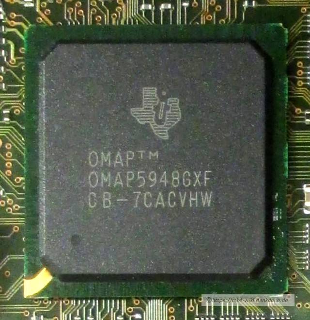
- Label:
OMAP5948GXF - Package:
BGA-289 - Vendor: TI (Texas Instruments)
-
- Praktisch baugleich mit OMAP5912 (sie OMAP1621, OMAP1611b) zzgl. ein paar „Kundenspezifischen Erweiterungen“ für BOSCH
- Datasheet and ressources: OMAP5912
- SRAM: 16 kbyte
- Boot ROM: 64 kbyte
- Erscheinungsjahr:
- DSP: C55x
- CPU (Core):
ARM926EJ-S- ARM Family:
ARM9E - ARM Arch:
ARMv5TEJ - Endianess:
Little Endian