Blackfin ADSP-BF561
Allgemeines
Der Blackfin ist ein Mikrocontroller, dessen Kern unter dem Namen Frio von den Unternehmen Analog Devices und Intel entwickelt wurde.
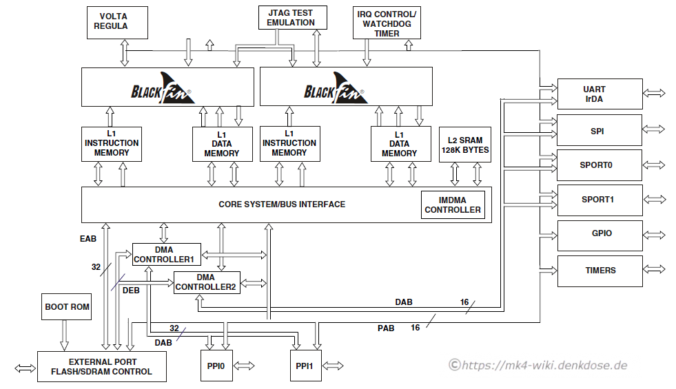
Er ist eine Kombination aus einem 32-Bit-RISC-Prozessor und einem 16-Bit-Festkomma-DSP mit zwei MAC-Einheiten mit SIMD-Fähigkeit. Dank umfangreicher Peripherieblöcke bieten sich verschiedene Einsatzbereiche an. Im Automobilbereich findet man Blackfin-Prozessoren hauptsächlich in Fahrerassistenzsystemen und in Infotainment-Applikationen.
Quelle Wikipedia: https://de.wikipedia.org/wiki/Blackfin
Datenblatt
FEATURES
- Dual symmetric 600 MHz high performance Blackfin cores
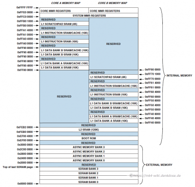
- 328K bytes of on-chip memory
- Each Blackfin core includes
- Two 16-bit MACs, two 40-bit ALUs, four 8-bit video ALUs, 40-bit shifter
- RISC-like register and instruction model for ease of programming and compiler-friendly support
- Advanced debug, trace, and performance monitoring
- Wide range of operating voltages, (see Operating Conditions on Page 20)
- 256-ball CSP_BGA (2 sizes) and 297-ball PBGA package options
PERIPHERALS
- Dual 12-channel DMA controllers (supporting 24 peripheral DMAs)
- 2 memory-to-memory DMAs
- 2 internal memory-to-memory DMAs and 1 internal memory DMA controller
- 12 general-purpose 32-bit timers/counters with PWM capability
- SPI-compatible port
- UART with support for IrDA
- Dual watchdog timers
- Dual 32-bit core timers
- 48 programmable flags (GPIO)
- On-chip phase-locked loop capable of 0.5× to 64× frequency multiplication
- 2 parallel input/output peripheral interface units supporting ITU-R 656 video and glueless interface to analog front end ADCs
- 2 dual channel, full duplex synchronous serial ports supporting eight stereo I2S channels
Memory Map
External (Off-Chip) Memory
The ADSP-BF561 external memory is accessed via the External Bus Interface Unit (EBIU). This interface provides a glueless connection to up to four banks of synchronous DRAM (SDRAM) as well as up to four banks of asynchronous memory devices, including flash, EPROM, ROM, SRAM, and memory mapped I/O devices.
The PC133-compliant SDRAM controller can be programmed to interface to up to four banks of SDRAM, with each bank containing between 16M bytes and 128M bytes providing access to up to 512M bytes of SDRAM.
JTAG
JTAG Frequency
There is a relationship between the JTAG frequency and the core clock frequency of the processor. The core clock should be at least twice the JTAG frequency in order for the JTAG interface to operate properly. If the core/JTAG clock relation is not followed, scan failures may prevent the emulator from connecting to the processor.
Bootstrap
The ADSP-BF561 contains a small boot kernel, which configures the appropriate peripheral for booting. If the ADSP-BF561 is configured to boot from boot ROM memory space, the processor starts executing from the on-chip boot ROM.
Watchdog
Each ADSP-BF561 core includes a 32-bit timer, which can be used to implement a software watchdog function. A software watchdog can improve system availability by forcing the processor to a known state, via generation of a hardware reset, nonmaskable interrupt (NMI), or general-purpose interrupt, if the timer expires before being reset by software. The programmer initializes the count value of the timer, enables the appropriate interrupt, then enables the timer. Thereafter, the software must reload the counter before it counts to zero from the programmed value. This protects the system from remaining in an unknown state where software, which would normally reset the timer, has stopped running due to an external noise condition or software error.
After a reset, software can determine if the watchdog was the source of the hardware reset by interrogating a status bit in the timer control register, which is set only upon a watchdog generated reset. The timer is clocked by the system clock (SCLK) at a maximum frequency of fSCLK.

