CP3CN37
FOTO
MPU Specs
- Manufacturer: National Semiconductor
- Marking: NS CP3CN37VVAWQ (CP3CN37-Serie)
- Package: LQFP-144
- 32K bytes internal RAM
- 16K bytes boot ROM
- Addresses up to 4M bytes of external memory using two chip select signals using 16 Bit data bus and 20 bit address bus
- Universal Serial Bus (USB) 2.0 On-The-Go
- Audio/telematics codec with dual ADC inputs and high-quality stereo DAC output
- CAN interface with 15 message buffers
- Serial bus interface (I2C comp)
- I2S digital audio bus interface
- Four UARTs
- Advanced Audio Interface (AAI)
- Two CVSD/PCM converters
- Timing and Watchdog Unit
- Up to 31 general-purpose I/O pins
- Operating voltage and I/O port operation at 3.0 - 3.3V
Datasheets
CPU
- CPU type: CR16C (CompactRISC, 16-Bit CPU)
- Endian: Little
- Registers: CR16 has 16 general purpose registers of 16 bits, and address registers of 21 bits wide. There are 8 special registers: program counter, interrupt stack pointer ISP, interrupt vector address register INTBASE, status register PSR, configuration register and 3 debug registers. Status register implements flags:
C, T, L, F, Z, N, E, P, I
The CR16 CPU was used in several National Semiconductor microcontrollers.
RESET
- External Reset—assertion of the RESET input (active LOW)
- Software Reset—enabled by writing special code sequences to the SWRESET register
- Timing and Watchdog Module (TWM)—overflow of the watchdog timer
- SDI Reset—reset from the Serial Debug Interface (SDI)
DEVELOPMENT SUPPORT
In addition to providing the features needed for the next generation of embedded products, the CP3CN37 devices are backed up by the software resources that designers need for rapid product development, including an operating system, peripheral drivers, reference designs, and an integrated development environment.
Texas Instruments offers a complete and industry-proven application development environment for CP3CN37 applications, including the IAR Embedded Workbench, iSYSTEM winIDEA and iC3000 Active Emulator, Development Board, and Application Software.
BOOT
The operating environment selects the reset vector (boot address). The operating environment is controlled by the states sampled from the ENV[1:0] pins at reset. Internal pullups on the ENV[1:0] pins select ERE16L mode if these pins are allowed to float.
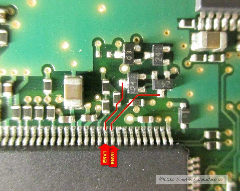
ENV0 = Pin 82
ENV1 = Pin 83
ENV[1:0] Operating Environment Reset Vector
00 ROM32 mode 0x00FE 0000
11 ERE16L mode 0x0040 0000
10 ERE16H mode 0x0080 0000
When the ENV[1:0] pins select the ROM32 environment, the reset vector is 0x00FE 0000, which is the start address of the on-chip 16K ROM.
An application which boots up in ERE16* mode can call the bootloader by jumping to 0x00FE 0000.
 On the BT-Module Board both pins are connected via small caps to VCC (+3.3V), thus making a bootmode of
 ERE16L, which means the chips starts off the external Flash which is mapped to start address 0x0040 0000.
The SWRESET(ISP) event invoked through the SWRESET register is intended to support softwareinitiated reset to the bootloader, however this is not enforced by hardware. To handle SWRESET(ISP) events in this way, the application must check the ISPRST bit in the MSTAT register. If this bit is set, an SWRESET(ISP) event occurred, and the application may jump to FE 0000h to pass control to the bootloader.
The bootloader does not distinguish between start-up from a hardware reset and an SWRESET(ISP) event, so it will perform the same clock configuration and host interface determination procedures in either case. If an application boots up in ERE16 mode and makes an unsuccessful attempt to reprogram the application software, it might not be possible to reboot into ERE16 mode. In this case, the system can be forced to execute the bootloader by pulling the ENV0 and ENV1 pins low during reset.
The ROM contains a bootloader which can be used to download and execute code in the on-chip RAM.
UART-BOOT: the bootloader monitors the four UART ports for activity. When signal transitions occur on a UART input, the bootloader measures the baud rate and waits for an ISP_HUNT_CONNECT_CLASSIC command. If this command is received within 1 second of detecting UART activity and determining the baud rate, the UART connection is used as the host interface.
USB-BOOT: if an USB enumeration process completes before the ISP_HUNT_CONNECT_CLASSIC command is received on a USB port, the USB connection is used as the host interface.
The bootloader is intended to support in-system programming (ISP) and other applications across a wide range of system designs. However, the bootloader only implements a minimal set of functions for downloading an application to on-chip RAM. To support a complete set of ISP functions, such as functions for programming Flash memory on the external memory bus, the host may download additional software to implement these functions.
So, CS0 für den externen Speicher geht an den /CS von Flash 3, rechts neben dem CP3CN37 auf der Platine. CS1 scheint nicht belegt. Somit ist klar das dieser 2 MByte große Flash die Software für den CP3CN37 enthalten muss. Habe den mittels TL866 ausgelesenen Dump angehangen.
Die Pins ENV0 und ENV1 sind nicht statisch belegt sondern werden über Transistoren geschaltet (siehe Bild). ENV0 ist dabei anfänglich LOW und wird nach ca. 1 Sekunde HIGH. ENV1 ist erstmal LOW und nach ca. 1 Sekunde sieht es aus als wäre doch eine hohe Frequenz. Laut Datenblatt hat der Pin mehrere Funktionen, u.a. PLL. Gut möglich das er nach dem Reset umkonfiguriert wird.
Aufgrund des Startmodus von ENV0 und ENV1 müsste der Chip also vom internen ROM booten. Dabei wartet er laut Datenblatt eine Sekunde lang ob auf USB oder UART etwas verbinden will. Das würde die oben gemessene Verzögerung erklären. Nach einer Sekunde werden die Pins dann für etwas ganz anderes umprogrammiert.
Nehmen wir an das ist so, dann stelle ich mir die Frage was nach dem ausführen des Bootloaders geschieht? Der ROM-Code ist laut Memorymap an Adresse 0xFE0000 und 16 KByte groß. Danach wird er irgendwo hinspringen, das ist aber nicht erwähnt. Ich vermute das er dann die Programmausführung ab 0x00 0000 beginnt, wie das sonst so übich ist? Ab dieser Adresse liegt dann das Flash. Also müsste ab dem Anfang valide RISC Maschinenbefehle stehen.
MEMORY MAP
The maximum memory size supported by the external bus is 2M bytes, because of the 20 address lines XA[19:0].
After reset, CSO will map external memory to address 0x0040 0000 and CS1 to 0x0080 0000.
The external program-flash of the module is connected to CS0.
JTAG
The Serial Debug Interface module (SDI module) provides a JTAG-based serial link to an external debugger, for example running on a PC. In addition, the SDI module integrates an on-chip debug module, which allows the user to set up to eight hardware breakpoints on instruction execution and data transfer.
The SDI module can act as a CPU bus master to access all memory-mapped resources, such as RAM and peripherals. Therefore it also allows for fast program code download using the JTAG interface
JTAG-Pins
FOTO
3.3V (IOVCC)
	TMS		59
	TCK		63
	TDI		58
	TDO		57
	/RESET	136
	GND		64
	IOVCC	65